The Photoresist and UV Exposure Method
Here are the steps for this method of DIY PCBs:
- Print your circuit design on transparent paper (transparency film for InkJet printers or laser printers)
- Place your printed design on top of copper circuit board that has photoresist film on it (like this one)
- Expose the board to UV light (UVA light to be specific, ideally in the 360-410nm range). The length of exposure depends on the intensity and proximity of the light.
- Wash away the exposed photoresist in positive developer solution (like this one)
- Immediately rinse it in water once it's done removing the unwanted photoresist. What you should have now is bare copper except for your circuit design, which should remain in green photoresist.
- Etch away the exposed copper areas with ferric chloride (like this one). Agitate the liquid until all of the unwanted copper areas have dissolved.
- Rinse the board in water again.
- Remove the remaining photoresist using acetone or nail polish remover. Your board is almost ready for soldering!
- Finally, drill holes everywhere your circuit calls for holes.
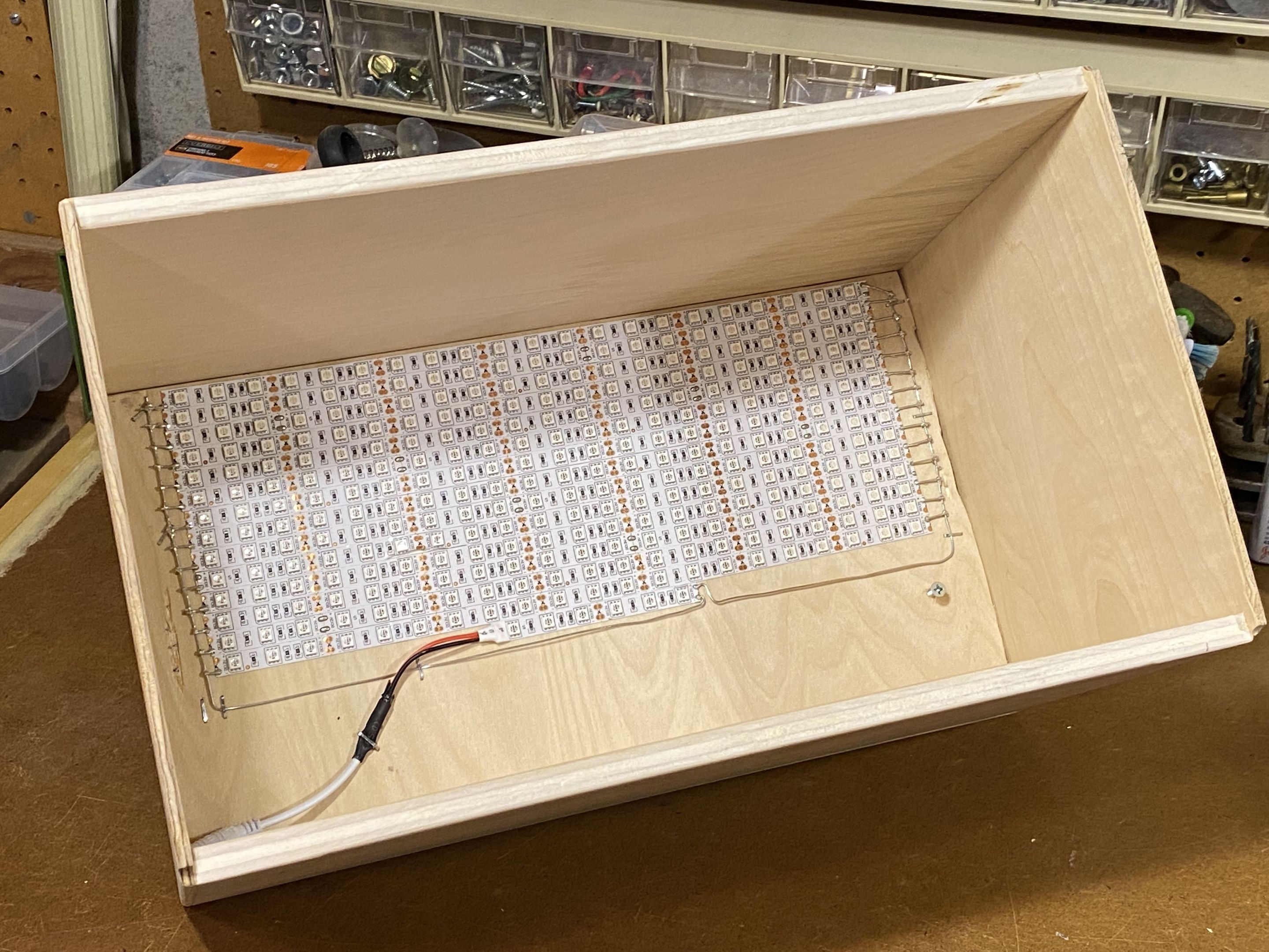
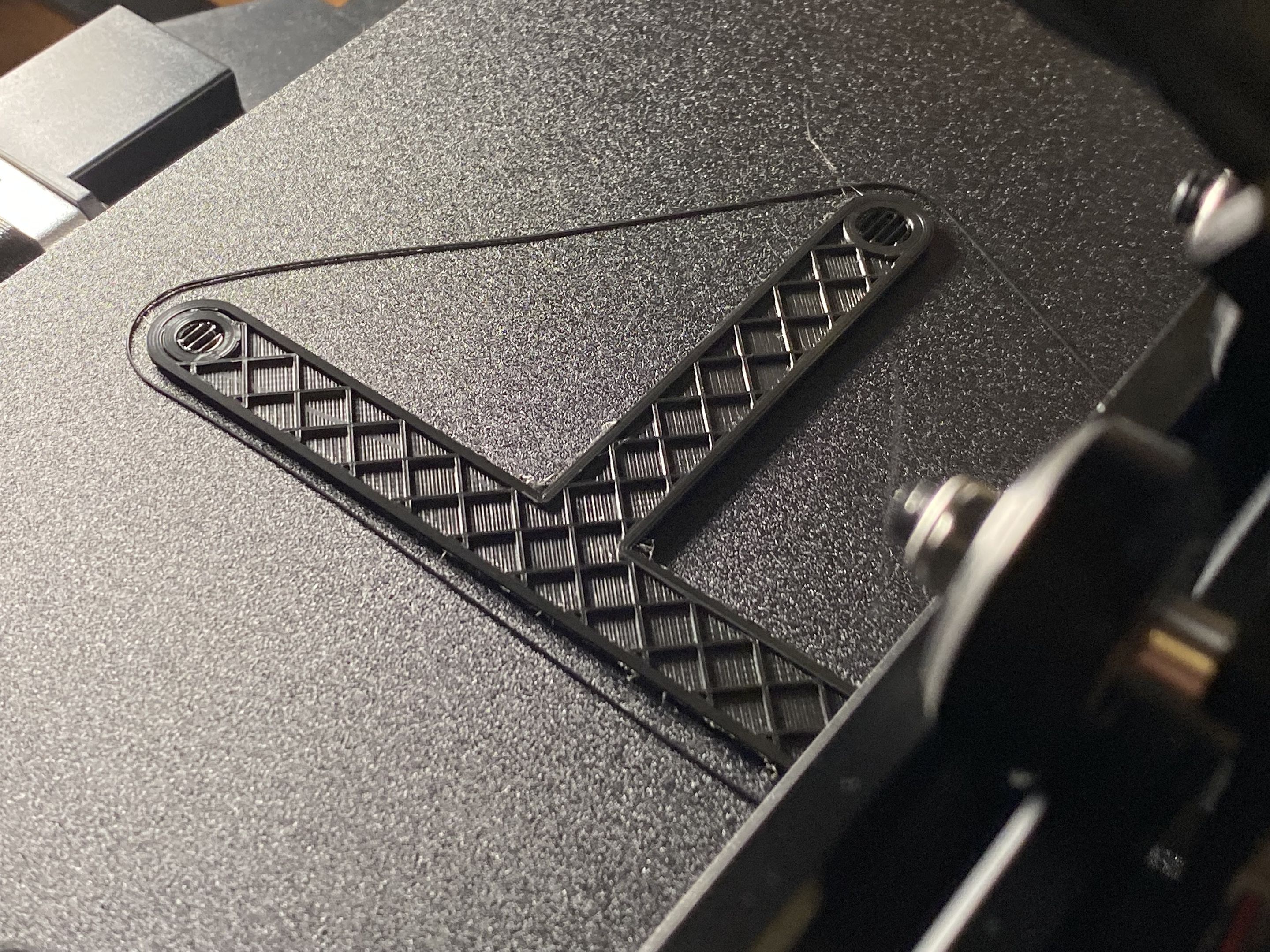
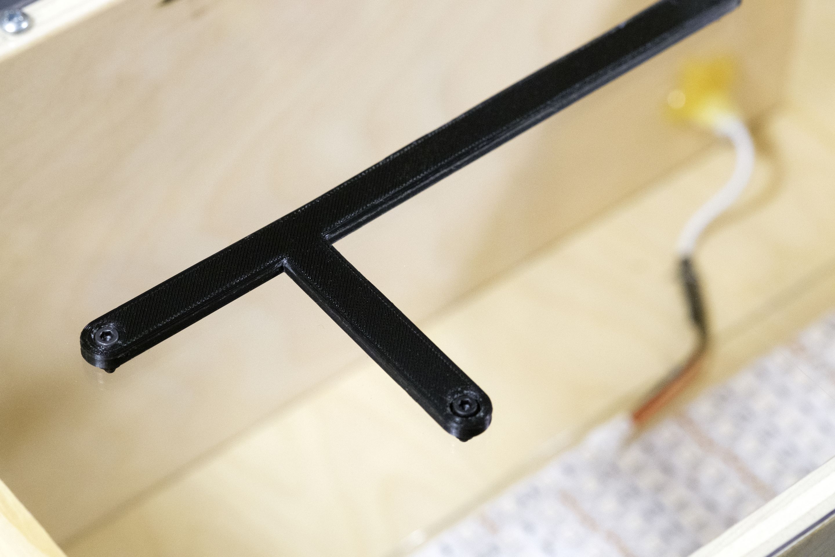
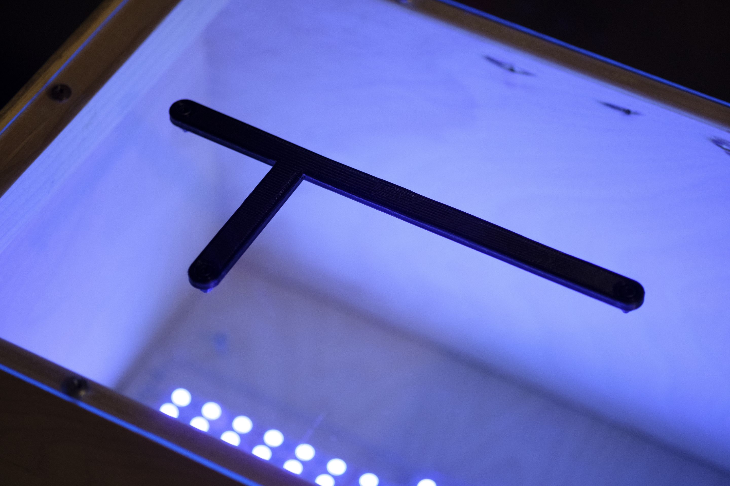
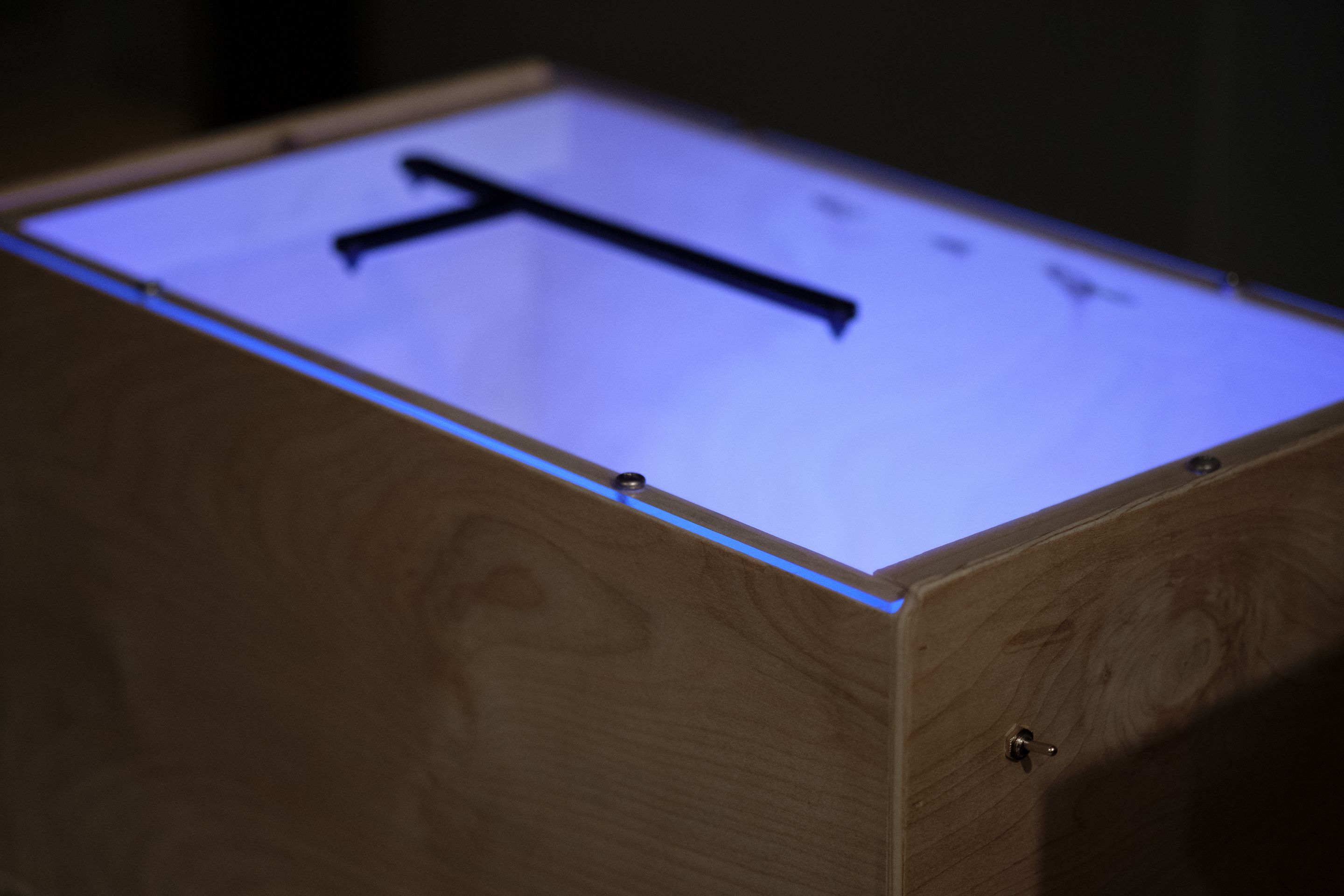
Building a UV Exposure Box
I bought a strip of 300 UV LEDs in the 395-405nm range (UVA) and built a box with a clear acrylic top and a 3D printed PCB alignment guide. This will allow me to consistently expose boards every time. But I'll still have to figure out what the ideal exposure time is.
Starting Small - Trial and Error
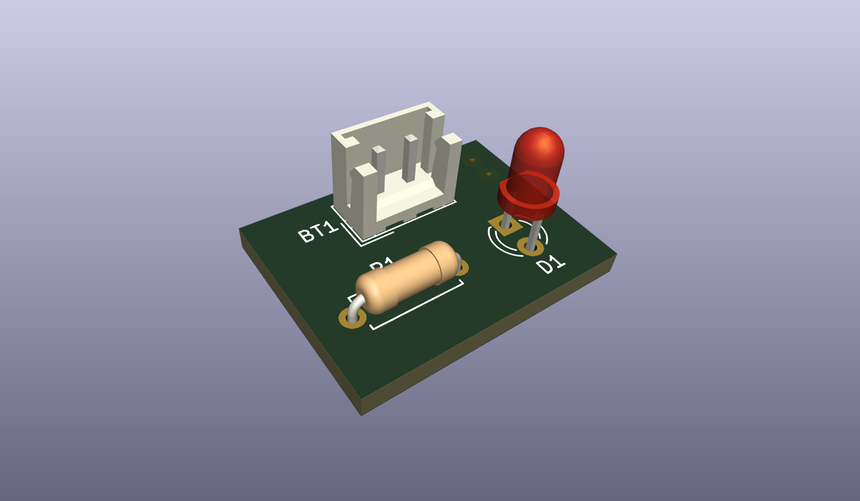
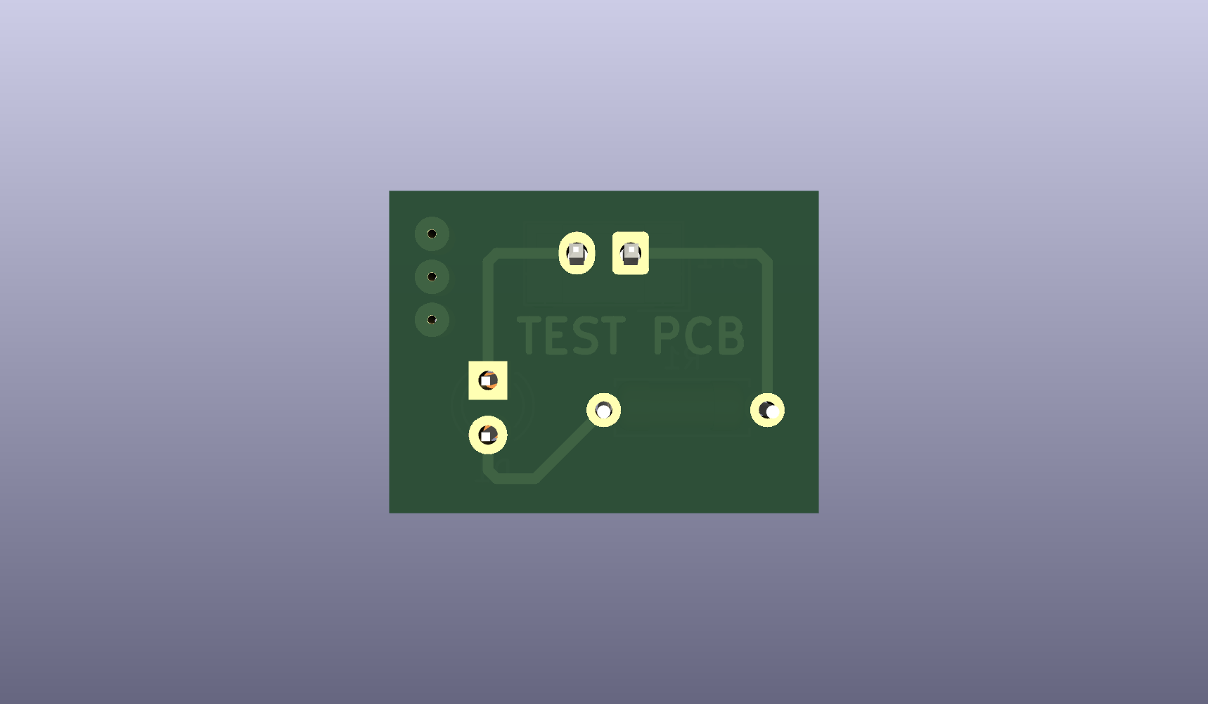
I didn't want to waste all of my copper board trying to figure out the optimal UV exposure time, so I designed a very small PCB in KiCad and printed it out on transparency film (see-through paper).
Next, I cut several small rectangles out of my larger 4-6" copper board. I used these little pieces to test different exposure times.
Exposure Times
First, I tried 5 minutes of exposure to my 300 UV LED array. The photoresist washed away completely when I placed it in the developer solution. Yikes. Too much exposure.
Then I tried 1 minute of exposure time. Same problem.
A More Methodical Approach
Then I tried a new method I learned about - cut a narrow strip of copper board and expose one portion of it at a time at specific intervals (10 second intervals for me).
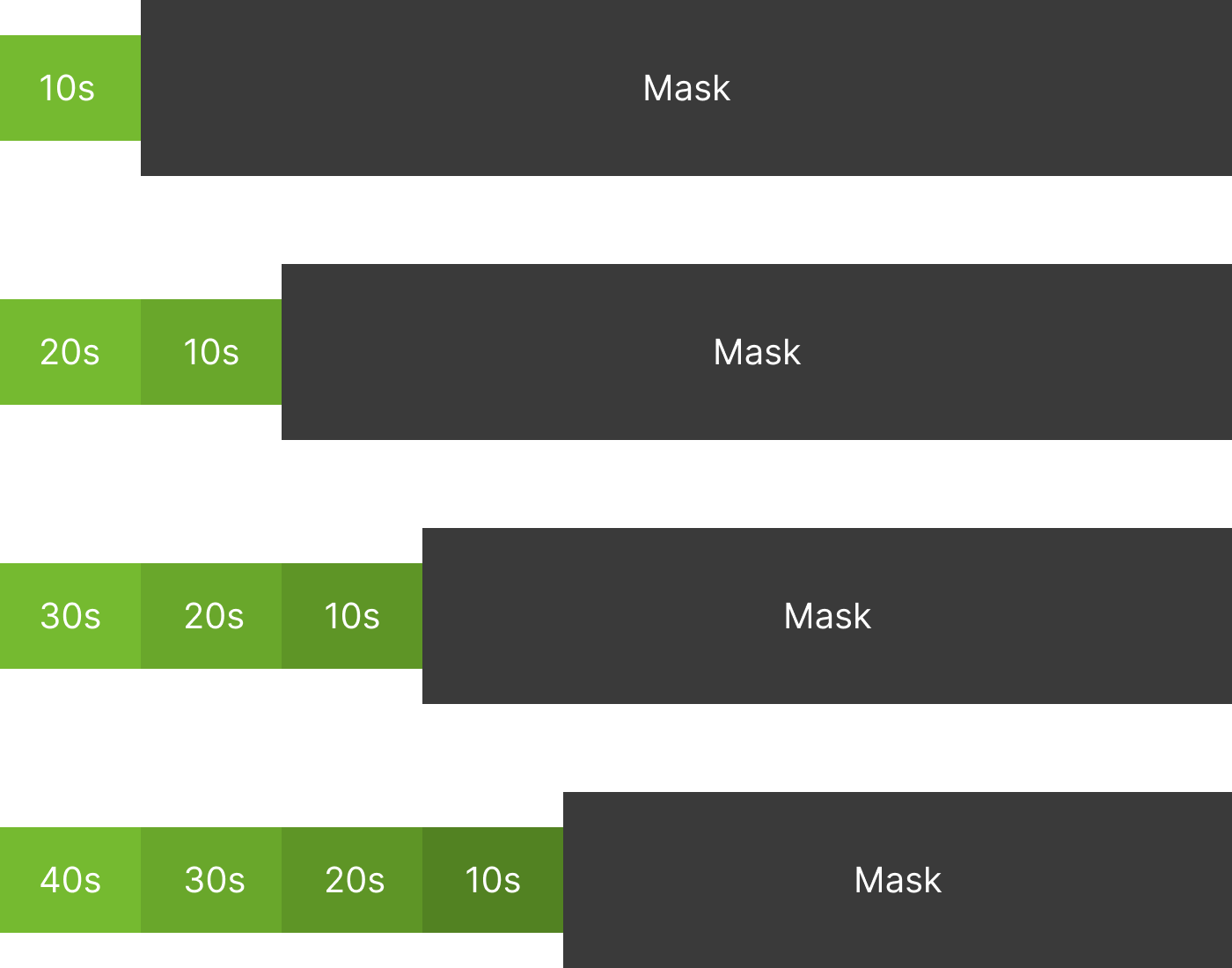
Then place it in the developer solution and see which amount of time results in an area that washes away versus remains protected with green photoresist.
This test led me to a seemingly ideal exposure time of 10 seconds. Holy crap. My UV lights are far more powerful than I thought.
I had read many mentions of 10-20 minute light exposure times, some using a regular light bulb, some using a blacklight, some using white LEDs, etc. But using 300 UV LEDs at an 8-inch distance apparently only requires about 10 seconds of exposure.
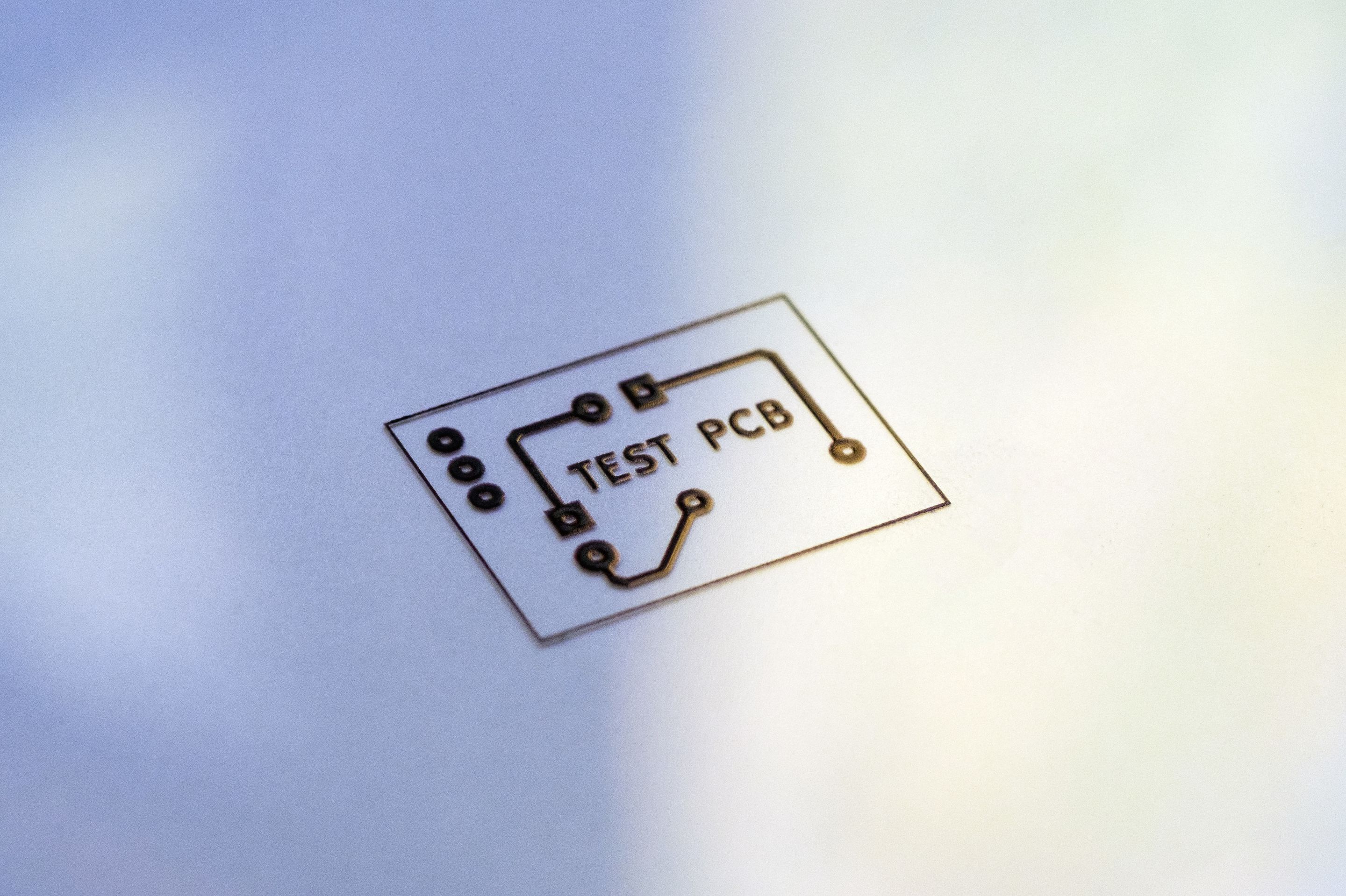
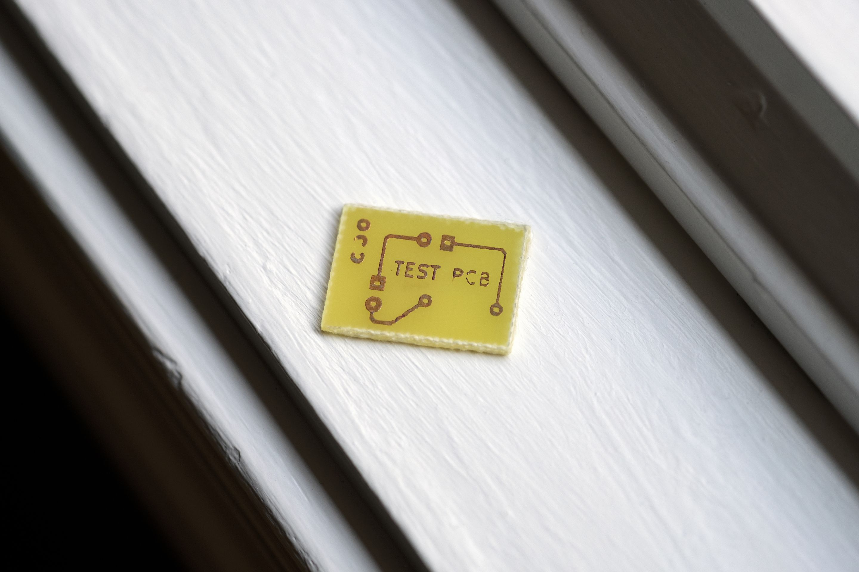
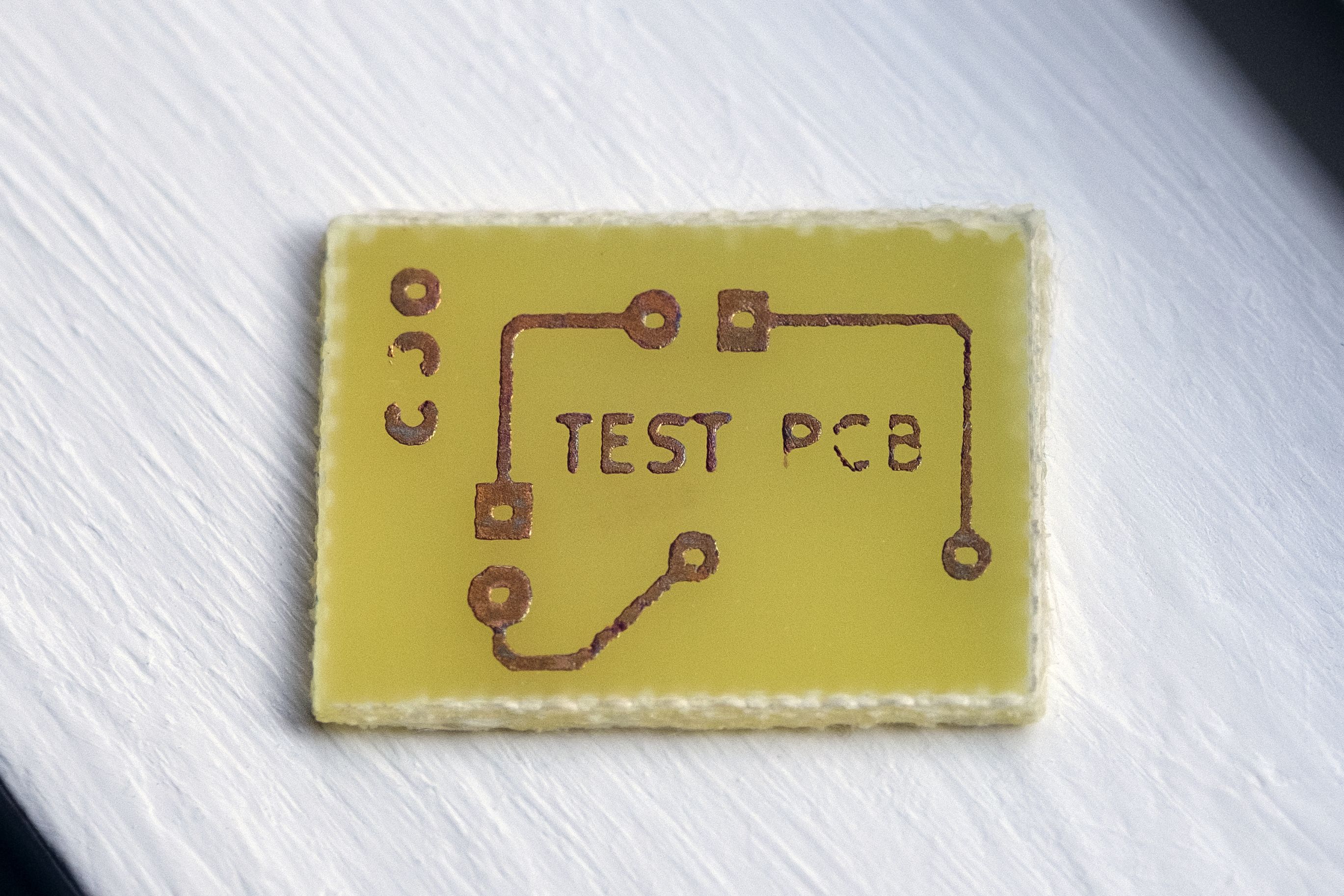
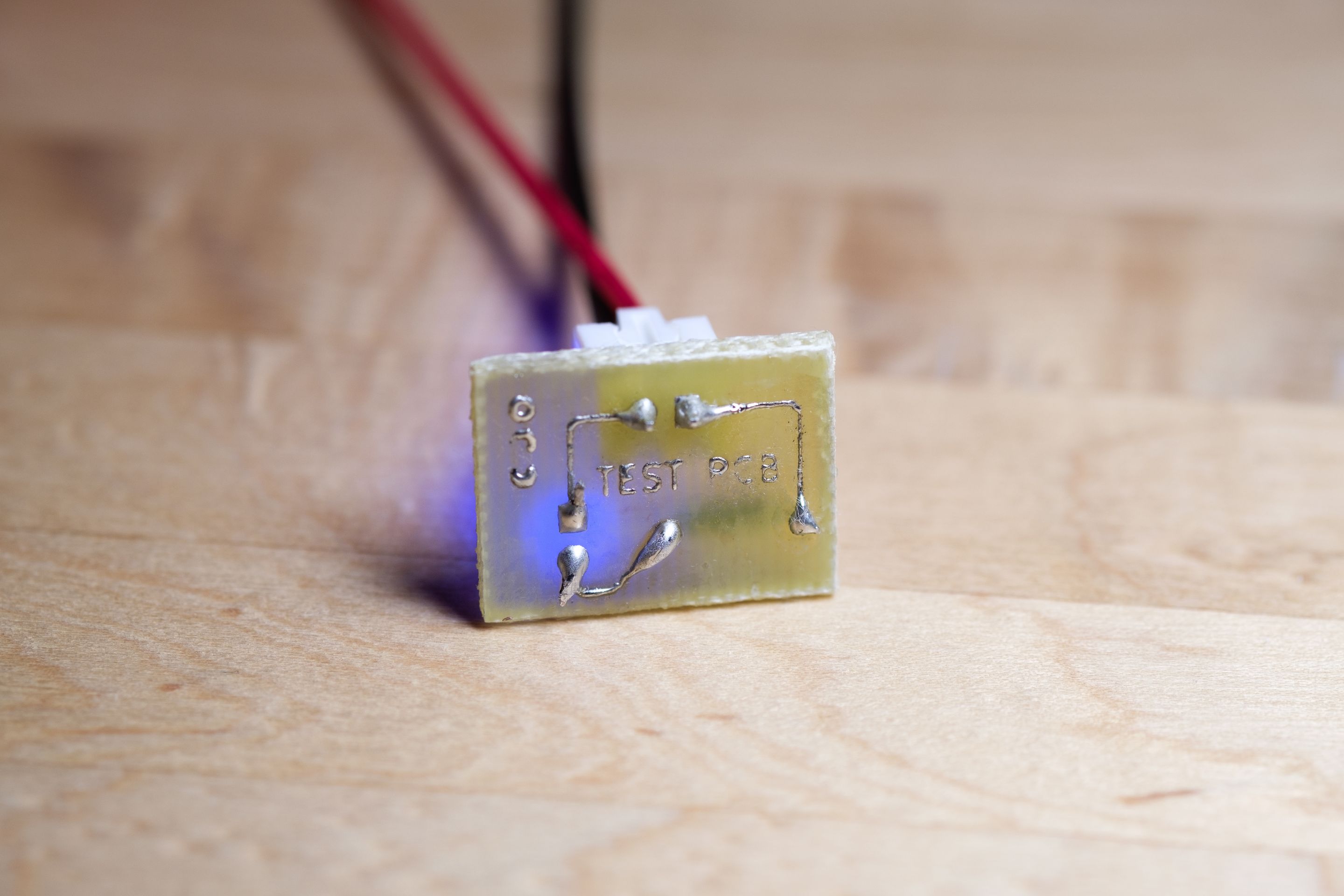
My First-Ever Homemade PCB
It's not perfect, but it could work! I'll drill some holes and solder on some components to test it out.
The copper traces are pretty thin and slightly worn. And a few of the test pads (not part of the circuit) on the left are half-dissolved. Either way, this is huge progress in only one night of iteration.
I think I need to double up my transparent design. The ink on the transparency film isn't very thick, so maybe stacking two designs on top of each other will help retain the copper traces better after exposure.
I'm also using a piece of clear acrylic (plexiglass) on top to press the design flat to the board, but I think it may need a little more weight to fully hold the design down.
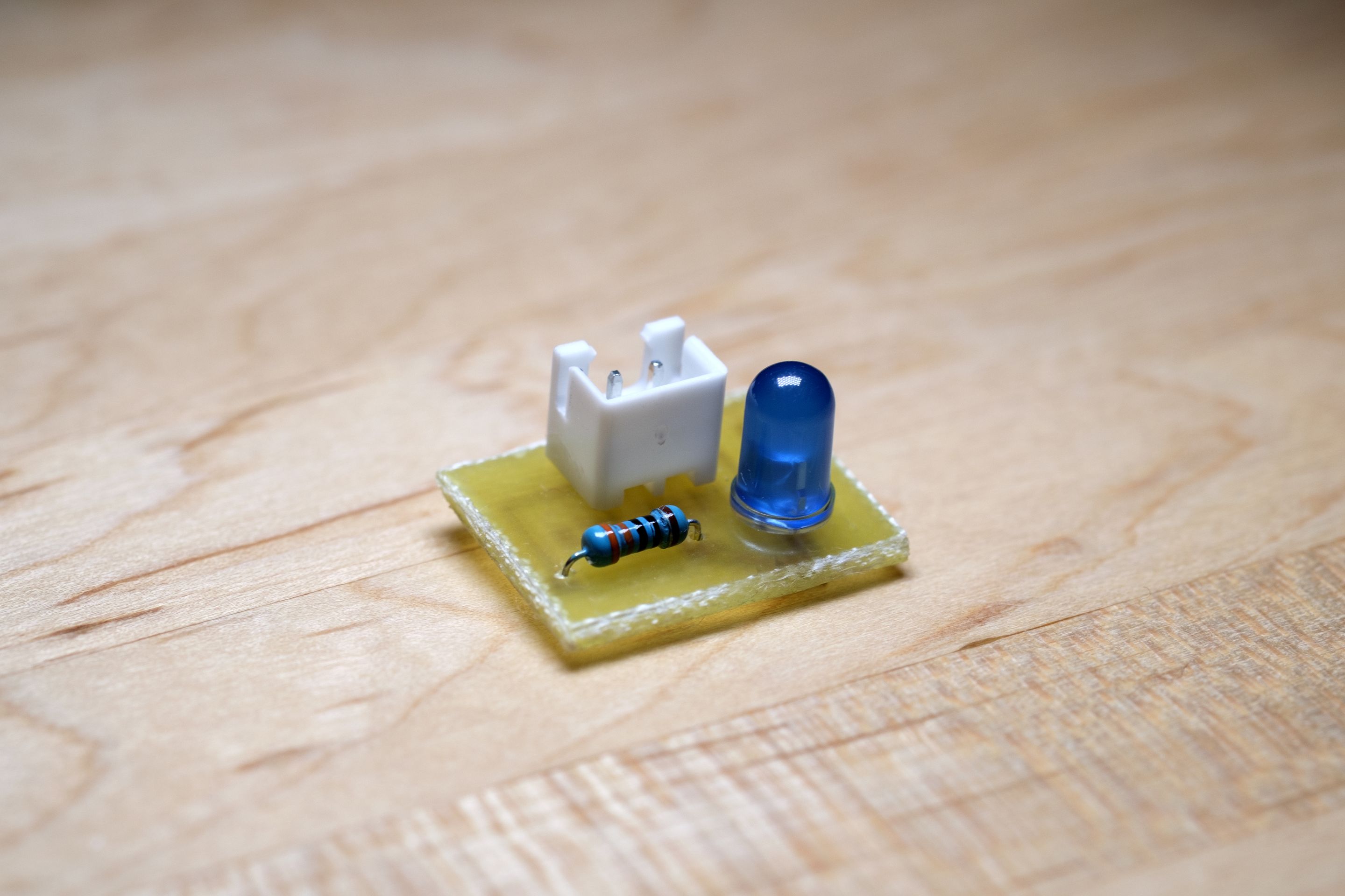
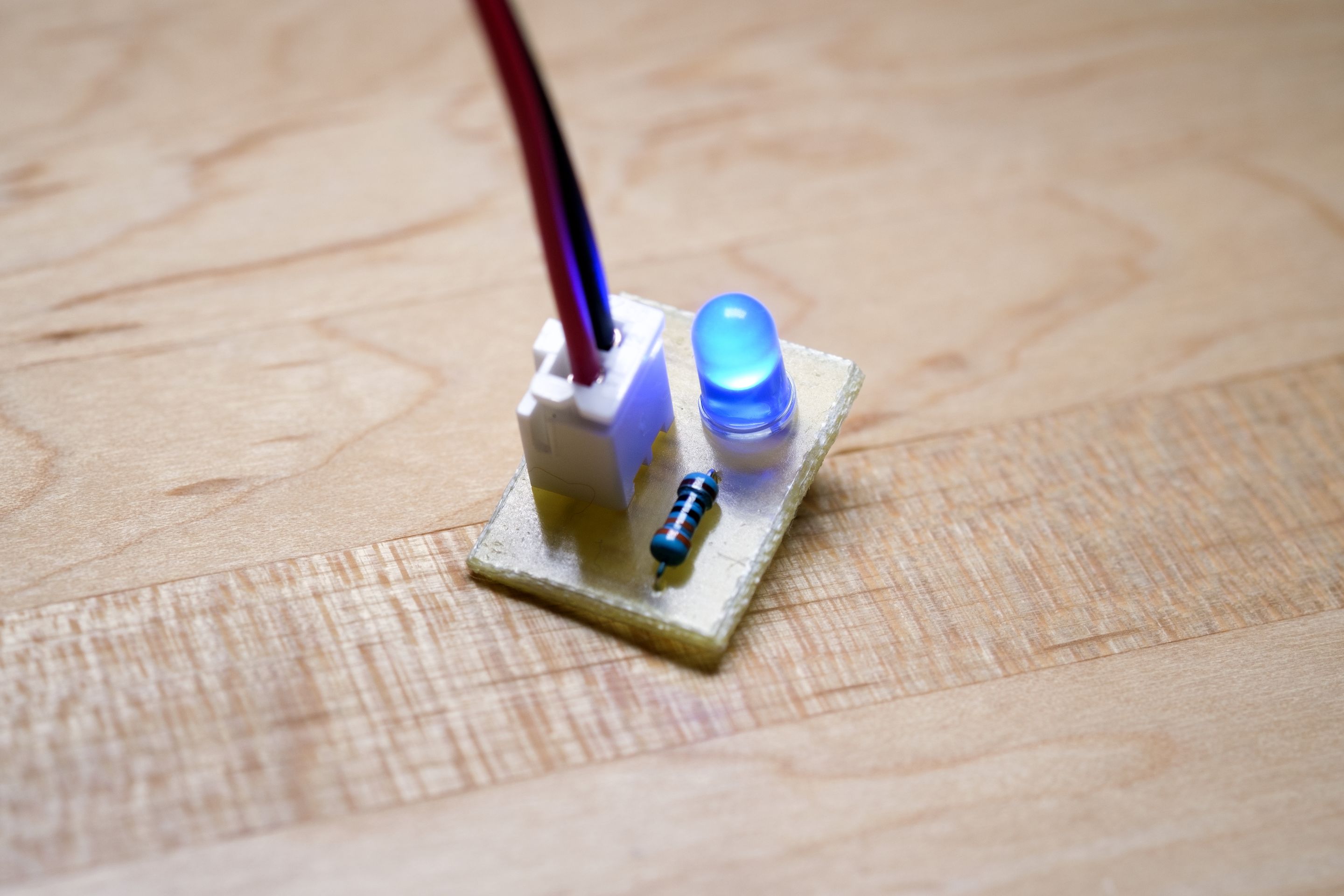
Soldering Up the First Board
It works! I'll still work to improve the quality, but I'm pretty happy with my tiny PCB. Little wins along the way keep me motivated to continue learning and iterating. That's why starting small is so important.
More to come as I continue experimenting...